DSP TU
RTTY seems like a great opportunity to learn a bit about digital signal processing.
I decided to use the PIC32MZ series of chips since I was most familiar with them.
The last 15 years of my career involved work with the PIC32MX.
|
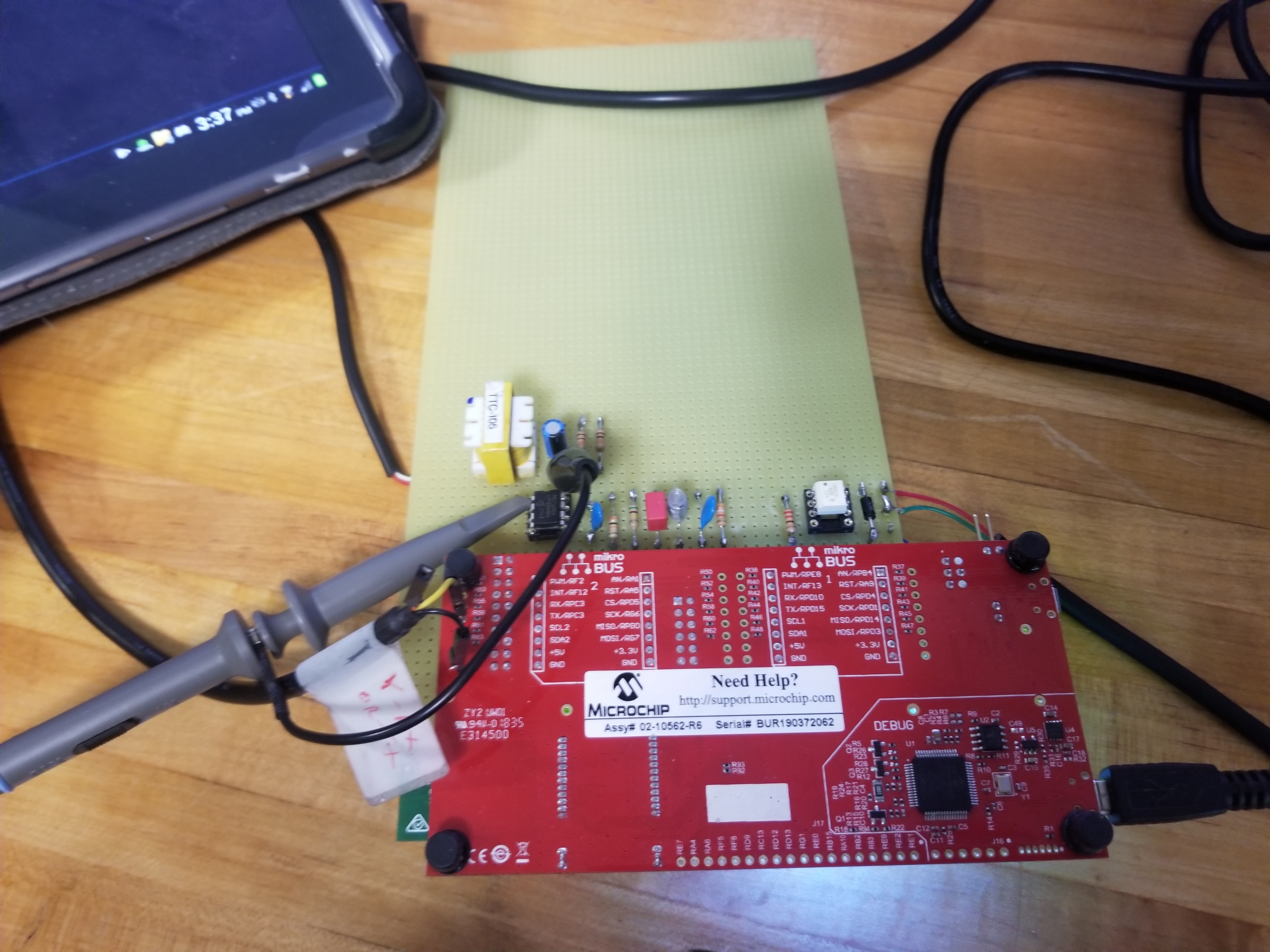
The first image shows the red
CURIOSITY PIC32MZEF DEVELOPMENT BOARD plugged into a piece of Vector
board that has the I/O circuitry (audio input and output analog circuitry,
loop keyer, etc.) wire wrapped. The transformer on the left of the Vector
board is the audio input transformer. It is being driven with audio from
here from the tablet computer
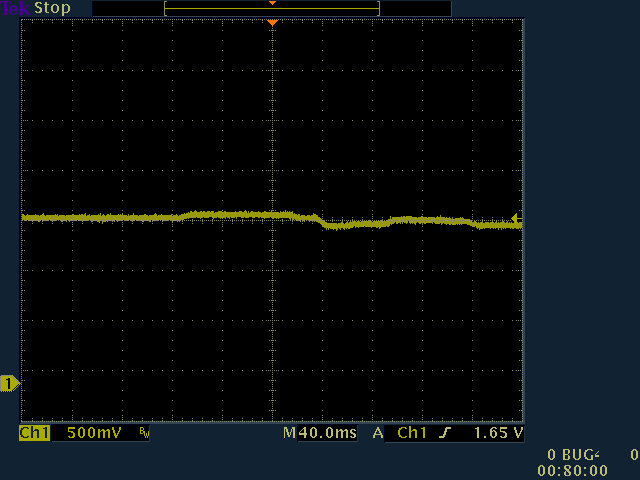
seen at the top left. The scope probe is connected to the audio output which
the firmware is directing the discriminator output to. The audio output
uses a PWM output from the PIC and passes it through a low pass filter to
recover the audio. The white chip on the right is an SSR keying the 60 mA
Teletype loop.
The second photo shows more of the development platform. A surplus
television is used as a computer monitor. The
MPLAB X software is on the screen with some of the code visible.
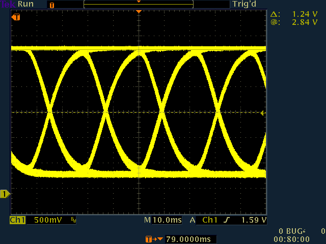
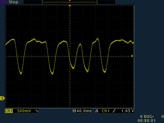
The scope is showing an eye pattern from the discriminator. Below the scope
is an audio mixer used to increase the audio level from the tablet computer
to drive the demodulator. |

|
The Terminal Unit consists of a modulator and a demodulator. The modulator seems like the simplest part while the demoduator
is more complex and needs to deal with noise, interference, and selective fading.
All DSP functions are done on a sample by sample basis (instead of using ping pong buffers and acting on the full buffer at once).
As long as all operations are completed before the next sample shows up, this should work. The sample rate is 8 kHz. All
calculations are double precision.
Incoming 12 bit unsigned integer samples are converted to a double precision floating point
with a value between -1.0 and +1.0 where -1.0 represents an analog input of 0V, and +1.0 represents full scale. Hardware
centers the audio between Vcc and GND.
Audio is output using PWM. The PWM frequency is 80 kHz. The PWM duty cycle is updated 8,000 times per second, corresponding with
the system audio sample rate. A sample value of -1.0 yields a duty cycle of 0%. A sample value of 0.0 yields a duty cycle of 50%.
A sample value of +1.0 yields a duty cycle of 100%.
Hardware
Audio Input
As shown in the sketch, the audio input is transformer isolated, then centered between ground and +3.3V, then applied
to analog input 4 on the PIC32MZ. Also shown here is a relay to drive the transformer with the AFSK output. The SEA245
transceiver uses a "tri-state" audio bus for audio in to and out of the transceiver. I currently have a Flesher
TU-170 driving this bus. I'll probably separate this out to two transformers, one input and the other output, to allow easy interface to other
transceivers. When using the SEA245, the input and output would just be placed in parallel.
Audio Output
The AFSK audio output is shown in this sketch. Since the PICMZ does not have a DAC, a PWM output is used instead.
The PWM frequency is 80 kHz, and the duty cycle is updated 8,000 times per second. The high PWM frequency makes it easier for the output LPF
to remove the PWM signal while passing the audio. Due to the high frequency and the relatively low GBW of the op amp, an RC filter is before
the active filter to remove much of the PWM signal. All calculations are done as double precision floats. When driving the PWM generator,
the double precision float is converted to duty cycle such that -1.0 outputs a 0% duty cycle, +1.0 outputs a 100% duty cycle, and 0.0%
outputs a 50% duty cycle. At the AFSK output, this represents a range of 0V, +3.3V, and 1.65V.
Loop Keying
As shown in the sketch, the look is keyed by a
G3VM-601BY solid state relay. The SSR is wired to "connection ADC with the two output FETs in series. This allows the connection to the loop
independent of polarity. The SSR supports a maximum load current of 100 mA, so it is suitable for the 60 mA Teletype loop. It can also
handle 480 V, so it does allows the magnetic field in the selector magnet to collapse very quickly on a mark to space transition. The
BZW04-342B transient suppressor diode limits the flyback voltage to 380 V (1 mA).
Loop Current Detection
The loop current detection is not yet built, but will probably use an H11AA1 optical
coupler. It has inverse paralell LEDs on the input, so it will not care about loop polarity. The LEDs will be placed in parallel with about
42 ohm resistor. This should result in 30 mA through the resistor and 30 mA through the LED (which is rated at a maximum of 60 mA). The loop
current sense will be in series with the loop keyer so a single 1/4 inch TRS plug can insert the TU into the loop.
Development Board Interface
The sketch shows the interface to the
CURIOSITY PIC32MZEF DEVELOPMENT BOARD.
Display Wiring shows the interface between the tuning display and the development board. The display uses SPI1.
Modulator
Data Low Pass Filter
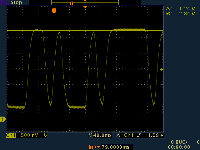
Data from the loop current detect opto coupler will cause the AFSK frequency to switch between 2125 (mark, loop current present) and 2295 (space, no loop current).
These values will be passed through a low pass filter to limit the keying harmonics. The output of the LPF will drive the DDS tone generator. The code for the
DDS tone generator accepts a frequency in Hz. The frequency will swing between the mark and space frequencies with a limited slew rate.
Direct Digital Synthesis Tone Generator
The DDS code calculates how many radians need to be added to the current
value on the next sample (125 us) to result in the correct frequency. On each call of DdsNextSample(), the code adds that value, corrects for overflowed
past 2*pi, then calculates the sine of resulting angle. The sine value is returned. This can drive the audio output (described above) to drive
the transmitter audio input.
Software
Code under development is available on GitHub.
MPLABX Project Configuration
Code is being developed using Microchip's
MPLAB X software. MPBABX includes a code generator called
Harmony. It generates code for initializing ports and peripherals. Since
most pins include multiplexers that allow a pin to serve one of several uses,
the Pin Configurator makes configuring the pins much easier than writing directly
to the corresponding registers. Harmony also includes a system clock configurator
to make sense of all the options for the system clocks. Harmony also generates
initialization code for peripherals along with interrupt code (such as for
timer 2 and the UART), and code to communicate with the peripherals. The next
several images show the Harmony configuration for the DSP TU.
| The image at the right shows the clock configuration as
set in Harmony. Note that we are using the 8 MHz FRC (fast RC) oscillator
to drive the System PLL to generate the 200 MHz system clock. The peripheral
clocks (such as timers and UARTS) are driven with 100 MHz. |
 |
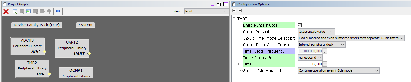
| The image at the right shows the configuration of timer 2.
It counts a 100 MHz peripheral clock. The configurator generates code
that sets the timer period register so it times out in 12,500 ns resulting
in a frequency of 80 kHz. The timer generates an interrupt that decrements
a software counter to count 10 timeouts resulting in the audio sampling
frequency of 8 kHz. Timer 2 drives OC1 (Output Compare 1) that is configured
to generate PWM for the audio output. The PWM is 80 kHz, and the duty cycle
is updated 8,000 times per second by the DSP code. |
 |
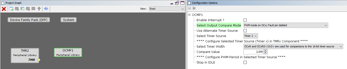
| The image at the right shows the configuration of OC1 (Output
Compare 1). It is configured to generate PWM based on Timer 2. It
does not have PWM fault inputs. Timer 2 is operating as a 16 bit timer
(not combined with timer 3 for 32 bits), so OC1 is also configured for
16 bits. OC1R is the output compare register, and OC1RS is the slave
output compare register. OCRS is transferred to OCR at the start of each
timer 2 cycle (when reset by the Period Register). This prevents PWM
glitches that would occur if the OCR register were written to directly (
for example, if timer 2 has a value of 2,000, OCR has a value of 3,000 but
is changed to 1,000, the OCR would not match timer 2 on this cycle resulting
in a 100% duty cycle for this one pulse.) |
 |
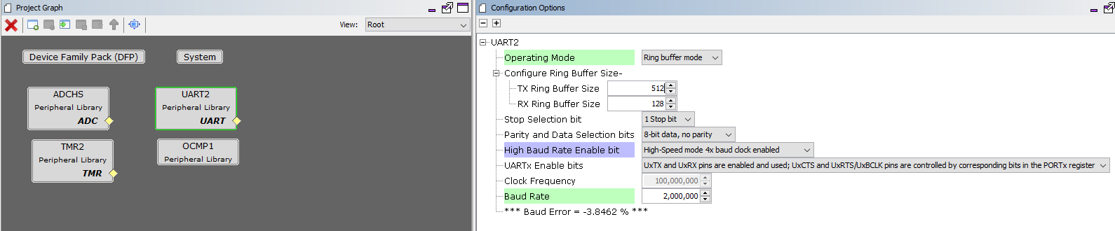
| The image at the right shows the configuation of UART2, which is used
for debug output. It is set to use a 512 byte ring buffer on the transmit
side so code is not slowed down waiting for each character to be transmitted.
Harmony generates the initialization code, the interrupt code to drive the
UART, and the code to put data into the ring buffer. The UART is configured
to use only the TX and RX pins. Handshake pins (CTS, RTS) are not used and
are free to be used for GPIO. The UART bit rate generator is driven by the
100 MHz peripheral clock and transmits at 2 Mbps. |
 |
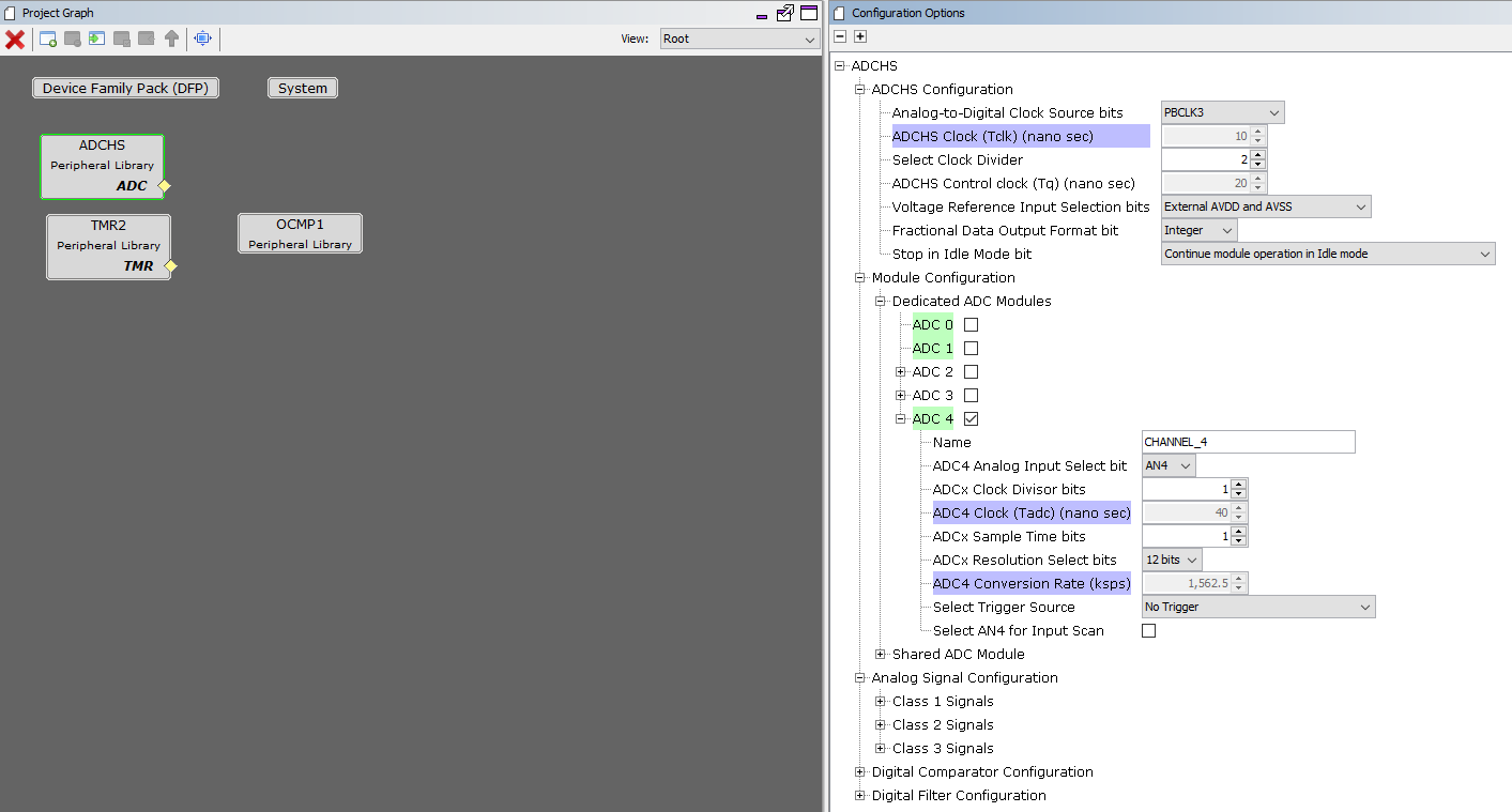
| The image at the right shows the configuration of the analog to
digital converter used for the AFSK input. Most settings are their default
values. Note that the power supply is used for the ADC reference,
the output format is unsigned integer, and the resolution is 12 bits.
The software starts an ADC conversion every 125 us, immediately after it
has retrieved the previous conversion so the next conversion happens
"in the background" while code is running instead of having to wait
for a conversion to complete. |
 |
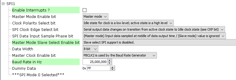
| The image at the right shows the configuration of SPI1 to drive the display. |
 |
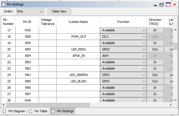
This image shows the configuration of several pins in the
Pin Configurator.
- RE8 is the PWM output driven by OC1 (output compare 1 which compares
timer 2 with a register value used to set the duty cycle).
- RB5 is LED_REDn, a GPIO output. The 'n' indicates it is active low.
Code clears LED_REDn to light the red LED and set it to extinguish it.
Similar definitions are used for the green and blue LEDs.
- RB4 is assigned to AN4, an input to an analog to digital converter.
This ADC digitizes incoming audio at 8000 samples per second. The ADC
completes a conversion much faster than is required. The code waits
for 10 timeouts of timer 2 (125 us), then reads the ADC, starts another
conversion, then runs the rest of the DSP code.
|
 |
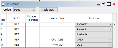
| The image at the right shows the pins assigned to the PWM output
(discussed above) and CPU_IDLEn. CPU_IDLEn is driven high at the start
of the DSP code and driven low at the end. The CPU load can be determined
from the duty cycle of this signal (8 kHz). |
 |
| The image at the right shows CPU_IDLEn, discussed above, and
DEBUG_UART2_TX. This is the transmit data output of UART2 which is configured
to transmit at 2 Mbps. Debug information is sent out this port when needed. |
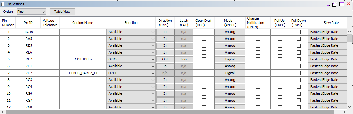 |
| The image at the right shows LOOP_KEY_OUT. This pin is driven high to
put the 60 mA current loop in the mark condition. It drives a solid state
relay that keys the loop. |
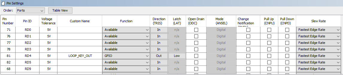 |
| The images at the right show the addition of the pins to drive the display over SPI. |
 |
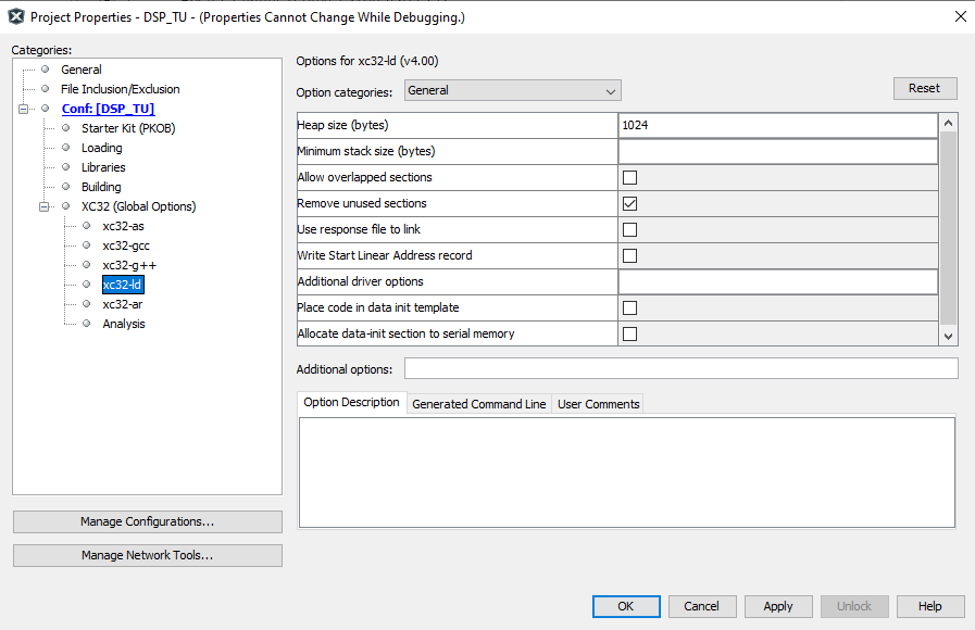
| The biquad filters store data on the heap. When the number of
cascaded filters in each of the tone filters was increased from one to
two, the heap overflowed. The image at the right shows the linker
properties where the heap was increased from 512 bytes to 1024 bytes. |
 |
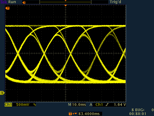
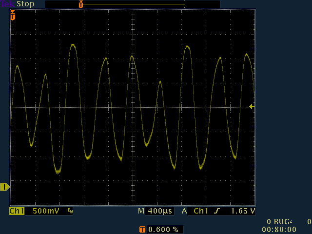
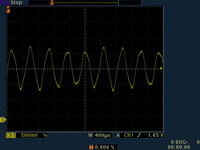
30 June 2022
Some tests were run with different filters. In the images below, the demodulator
was driven with random 22 ms per bit audio with space 20.8 dB below mark
to simulate selective fading. The audio is
here. The audio
output of the DSP TU was "connected" to the discriminator output. The eye
diagrams below are the results. The audio output is 0V for a sample value of -1.0
and +3.3V for a sample value of +1.0V. Therefore, +1.65V corresponds to a sample
value of 0.0. The scope is adjusted to place +1.65V on the center graticule.
Software duplicate of Flesher
TU-170. The data crossover points are on the 0.0 point, so we have no bias
distortion.
- Pre-Limiter Filter: None
- Limiter: Uses copysign() function. If sample is positive, output is +1.0.
Otherwise, sample is -1.0.
- Tone Filters: Each tone filtered by 3 biquads, each with Q=13 for overall
Q=25 and bandwidth of 83 Hz
- Data LPF: 45 Hz 2 pole
| 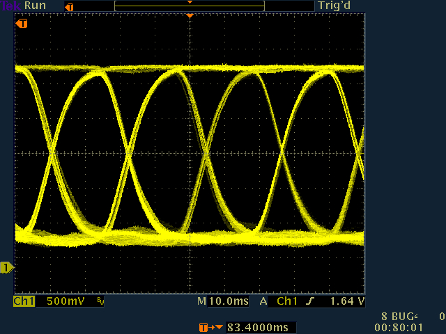 |
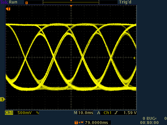
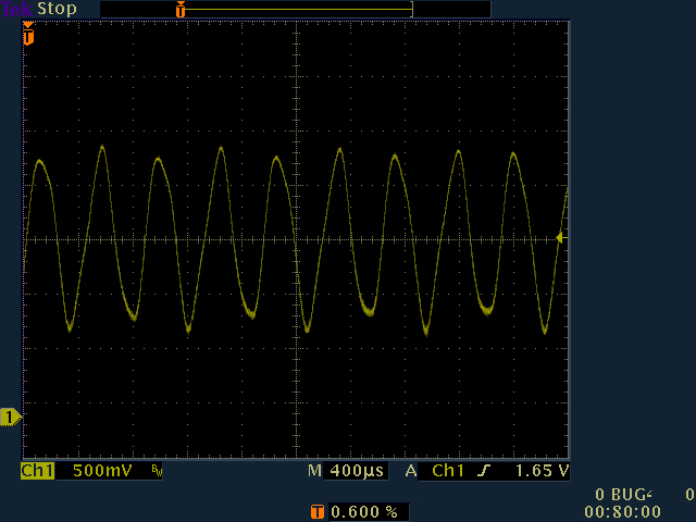
The tone filters here are narrower than those suggested in
Filters for RTTY. The eye is open, but alternating bits do not
reach the full discriminator output. If successive bits are the same,
the full output is reached. The data crossover points are on the 0.0 point, so we have no bias distortion.
- Pre-Limiter Filter: None
- Limiter: Uses copysign() function. If sample is positive, output is +1.0.
Otherwise, sample is -1.0.
- Tone Filters: Each tone filtered by 2 biquads, with each with Q=40.5.
Overall Q is Qn / sqrt (2^(1/n) -1) = 63 and bandwidth
of about 30 Hz. See
Cascaded BPF
Calculator. This is less than the recommended tone filter bandwidth
of 54.545 Hz.
- Data LPF: 27.27 Hz 2 pole
| 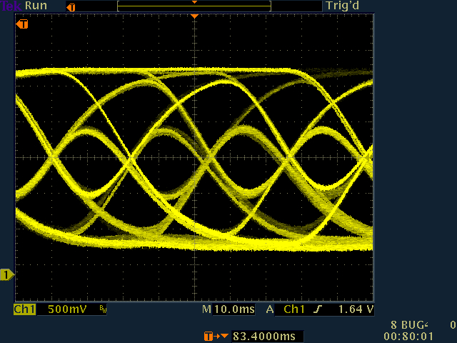 |
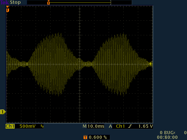
Same as above, tone filters are single biquads so bandwidth is closer
to ideal. The wider bandwidth lets single bits reach a higher voltage.
- Pre-Limiter Filter: None
- Limiter: Uses copysign() function. If sample is positive, output is +1.0.
Otherwise, sample is -1.0.
- Tone Filters: Each tone filtered by 1 biquad with Q=40.5 and bandwidth
of 52.5 Hz
- Data LPF: 27.27 Hz 2 pole
| 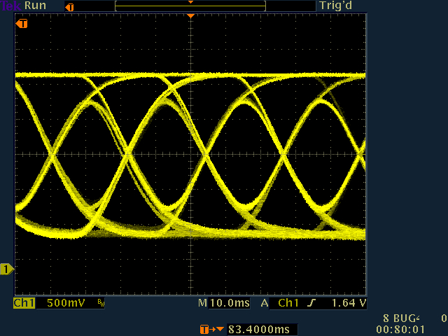 |
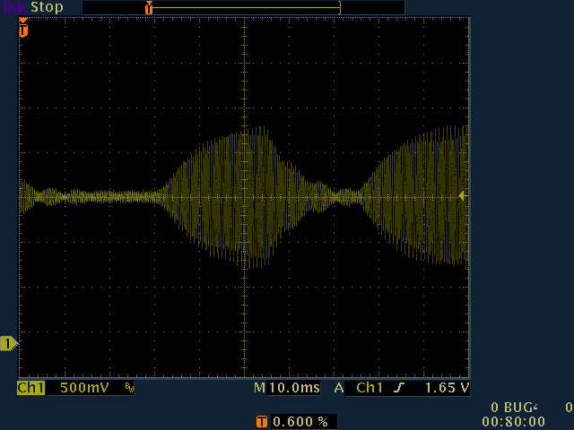
Same as above, but a bandpass filter is added in front of the limiter.
TU Notes showed no bias distortion
due to pre-limiter filtering and selective fading with Q=10, but substantial
bias distortion with Q=20.
- Pre-Limiter Filter: FC=2208.365 Hz, Q=10
- Limiter: Uses copysign() function. If sample is positive, output is +1.0.
Otherwise, sample is -1.0.
- Tone Filters: Each tone filtered by 1 biquad with Q=40.5 and bandwidth
of 52.5 Hz
- Data LPF: 27.27 Hz 2 pole
|  |
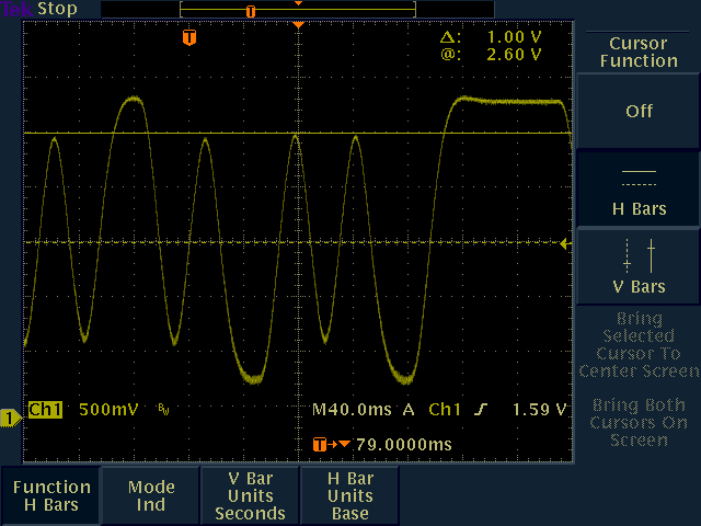
Running the test described here,
about 68 error-free lines were received. This is about the same as the TU-170
and the DSP copy of the TU-170.
2 July 2022
All the below tests were done with
this audio,
random data with 22 ms per bit and space 20.8 dB below mark to simulate selective
fading.
- Pre-Limiter Filter: FC=2208.365 Hz, Q=10
- Limiter: Uses copysign() function. If sample is positive, output is +1.0.
Otherwise, sample is -1.0.
- Tone Filters: Each tone filtered by 2 biquads each with Q=20 for
overall Q of 31 and bandwidth of 68 Hz.
Filters for RTTY suggests 3 pole
Butterworth tone filter
bandwidth of 1.2 * BaudRate (1.2 * 45.45 = 54.545 Hz).
- Data LPF: 27.27 Hz 2 pole
Note that single bits do not reach the same voltage as successive bits.
The second image shows a few successive bits. When more than one bit in
sequence is the same, the mark (positive) excursion is 1.30V above
+1.65V, which represents 0.0 discriminator output. If bits alrernate,
(where the horizontal cursor is set), the voltage is +1.0V above. For
negative (space) excursions, successive identical bits results in an
excursion of -1.26V, while alternating bits have an excursion of -0.890V.
Since both the tone and data filters do not have a rectangular
frequency response, there is some attenuation of the keying sidebands in
the tone filters and harmonics in the data low pass filter, both limiting
the slew rate of the data. Perhaps the bandwidth and cutoff frequency should
be increased so alternating bits can reach the same excursion as successive
identical bits.
| 
 |
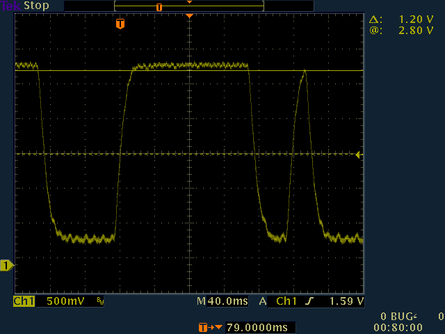
The slow rise time resulting in less than full excursion on single
bits could be due to the pre-limiter filter, the tone filters, or the
data low pass filter. It appears that the major contributor is the data
low pass filter. Disabling the pre-limiter filter made no difference. The
image to the right is with the following settings.
- Pre-limiter filter Q = 10
- Number of cascaded biquads in each tone filter: 2
- Tone filter biquad Q (each biquad): 20
- Tone filter overall Q: 31
- Tone filter bandwidth: 68.4 Hz
- Data LPF cutoff frequency: 150 Hz
The single bit excursions almost reach the multibit excursion. With
the data LPF at 150 Hz, the excursion limit is due to the tone filter Q.
Also with this data LPF, ripple is visible. This is two times the tone
frequency due to the full wave rectification (absolute value) used in
the envelope detection.
The tone filter Q and data LPF cutoff frequency were adjusted so the
peak excursion was about the same for single bits and sequential bits.
The last two images (single sweep and eye diagram) were with the
following parameters.
- Pre-limiter filter Q: 10
- Number of cascaded biquads in each tone filter: 2
- Tone filter biquad Q (each biquad): 18
- Tone filter overal Q: 28
- Tone filter bandwidth: 76 Hz
- Data LPF cutoff frequency: 50 Hz
Having each bit result in the same excursion should allow us to
capture the maximum excursion during each bit to determine a
dynamic threshold. |
 |
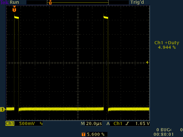
| To get an idea of how heavily loaded the CPU is, RE7 is driven
high when the DSP code is entered (every 125 us), and set low when the
code is exited. The code then loops until the next 125 us time is up
(timer 2 running at 80 kHz and a software counter counting 10 timer 2
timeouts for a sampling frequency of 8 kHz. The 80 kHz is the raw PWM
frequency on the audio output. The duty cycle is updated 8,000 times
a second. The image at the right shows that the CPU is spending about
3.7 percent of the time executing the DSP code. There is some interrupt
code not included in this, but it is minor (timer 2 timeout decrementing
a software counter). The code running is that described above plus the
DDS tone generator. | 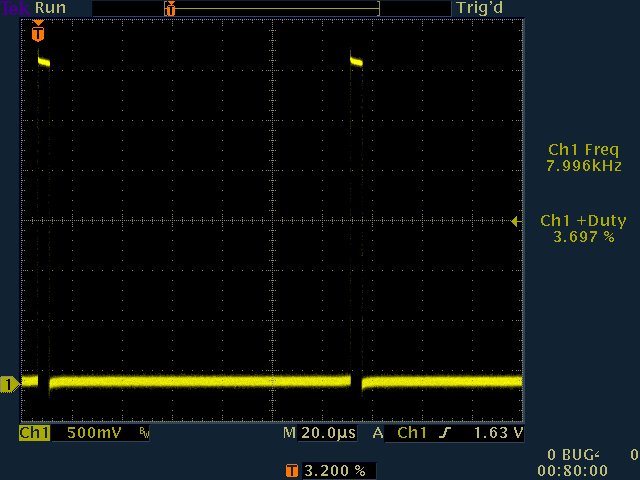 |
5 July 2022
|
Lots of changes of the last few days! First off, when the project was previously
renamed to DSP_TU, some files and directories changed, but not all. After spending
a couple days trying to fix it, I created a new project named DSP_TU, went through
all the configuration (see Harmony at the top of the software section) and copied
the source code files into the new project. It finally looks good!
Added an
AGC
after the input filter. This is a simple AGC that compares the full wave
rectified and filtered level to a target level and applies a gain. To keep
it from running away, a maximum gain is specified.
Added
Dynamic Threshold Control. similar to "slideback" compensation as discussed
in A New Approach to TU Design Using a Limiterless Two-Tone Method. The analog
circuitry discussed there provided a threshold (actually biased the bipolar
envelope) such that the mark/space switch was half way between the peak mark and
space voltages. The "slideback" voltages were held in capacitors that quickly
charged to the peak mark or space envelope voltage and slowly discharged to
follow the varying peak envelope voltage. This approach had a problem with hand
keyed RTTY since there was a long delay between space signals which would adjust
the threshold as though the space envelope was low. In this software version,
as each bit is received, a maximum level is determined. The threshold is
(MarkMax - SpaceMax)/2 passed through a low pass filter. The low pass filter
keeps the threshold from changing instantly on each bit but, ideally fast enough
to deal with selective fading. Originally, the code compared the current
MarkLevel-SpaceLevel to the LastThreshold (that which was last calculated) to
determine if the received signal was mark or space so the maximum level calculation
ended up properly in a max for mark or space. However, if the LastThreshold
gets messed up (so that MarkLevel-SpaceLevel) never crosses the threshold, the
threshold updating stops. For that reason, the mark/space decision here is done
just based on which level is higher.
The various parameters were adjusted. With a maximum AGC gain of 50 and a
dynamic threshold low pass filter cutoff of 50 Hz, the test described
here resulted in about
84 lines printing correctly. This is quite a bit better than DSP TU 220615 on
that page (67 lines correct, the same as the
Flesher TU-170).
The overall design at this point is:
- Input Filter: Q=10
- AGC: LPF F=1.0 Hz
- Limiter: none
- Tone Filters: 2 stages, Q of each 18.0. Overall Q=28, BW=76 Hz
- Envelope Detect Data Low Pass Filters: FH=50.0 Hz
- Dynamic Threshold Control Filter (how fast threshold can change): 50.0 Hz
|
Analog to digital converter output.
Output of the input bandpass filter.
Output of the automatic gain control.
Output of the mark tone filter.
Output of the space tone filter.
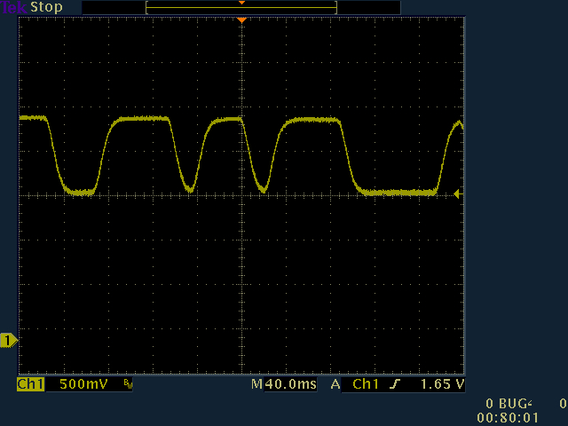
Output of the mark demodulator (full wave
rectifier followed by data LPF).
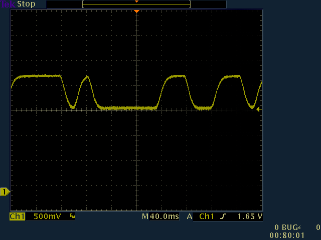
Output of the space demodulator (full wave
rectifier followed by data LPF).
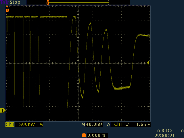
Output of the discriminator (mark demod
minus space demod) at tone start. Initial clipping due to high AGC gain.
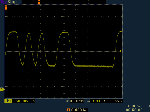
Output of the discriminator (mark demod
minus space demod) once the AGC adjusts to the input level.
Output of the dynamic threshold detector.
The TU was fed with real RTTY received over an SDR so there would be some
selective fading.
Discriminator less dynamic
threshold. Above 0.0 (center scale) should be mark and below space.
The TU was fed with real RTTY received over an SDR so there would be some
selective fading.
Discriminator less threshold
fed with random 22 ms data to generate eye pattern.
With the added code, the CPU load has increased
to about 5%.
|
6 August 2022 - Tuning Scope
|
This commit adds an XY tuning scope to the terminal unit. The output of the mark BPF causes deflection in the X direction, while the output of the space BPF causes
deflection in the Y direction.
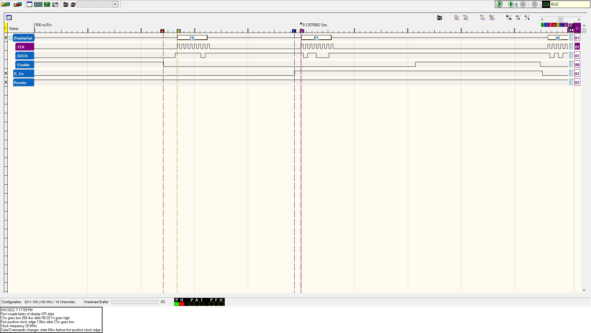
The display is a 128x128 OLED display with an SPI interface. The display comes with no doucmentation
other than it uses the SSD1351 controller. The SSD1351
supports a wide variety of displays and has registers that are set up during initialization for that particular display.
buyDisplay.com offers a similar display,
also a 150x150 OLED display with the SSD1351 controller. There is also little documentation for that
display, but they DO provide 8051 demo code. That code bit bangs the SPI and drives CSn high
after each transmitted byte, which conflicts with the datasheet where CSn is held low through the
whole transaction (command and data).
The display can operate as either a 3 wire or 4 wire SPI device. The display is write only, so the MISO input of the SPI port on the PIC is not used. In 4 wire mode, the
wires are CSn (active low chip select), clock, MOSI, and Data/Commandn. Data/Commandn is low for the first byte of a command and high for the following data bytes.
The display can also operate in a 3 wire mode. In this mode, each byte is transmitted as 9 bits with the first bit being the DataCommandn bit. It is low for the first byte
of the command and high for the remaining data bits. Since the PIC does not support 9 bit SPI, the 3 wire mode was not used.
The hardware SPI1 module in the PIC32 is used to drive the display. The SPI clock runs at 25 MHz. To avoid having the system wait for the transmission of each byte over SPI,
a large 16 bit wide FIFO is used. The lower 8 bits contain the byte to be transmitted over SPI. The upper 8 bits hold the state of the Data/Commandn line for this byte along with
with the state of the CSn line. The buffer holds all the information to properly transmit a byte. The main loop polls the SPI in a loop pass where there was no audio sample
to process. The SPI poll checks to see if the SPI port is busy. If not, it checks to see if there is data in the FIFO to transmit. If so, it sets CSn and Data/Commandn as
indicated in the high half of the FIFO word, then puts the low half in the SPI transmit buffer. If the buffer entry has CSn false, the low byte is not transmitted. See
DisplayPoll() in display.c for details.
To allow the display to be blanked, the display FIFO has to be relatively deep. The display address pointer is set to the first position on the display, then black is
written to 128 lines and columns (16,384 pixels). Writing each pixel takes three bytes (the command followed by the 16 bit color as shown below). This requires the FIFO to be
about 49,000 words deep (recall that each 16 bit word holds the 8 bits of data to be sent along with the state of the chip select and Data/Commandn pin). The FIFO depth is set
to 70,000 in display.c. Since the FIFO is on the heap, the heap size had to be increased to
200,000 bytes.
The format of the color data sent to a pixel is also not documented. Through experimentation, it was determined that each pixel color is a 16 bit values with the bits
assigned as:
- b15..b11 - Red
- b10..b5 - Green
- b4..0 - Blue
DisplayWriteNextPixel accepts 8 bit red, green, and blue values. The bits are values are shifted right such that the msb of the incoming parameter corresponds with the msb
of the color component sent to the display.
The addition of the display code increased the CPU utilization from the previous 5% to about 12%.
|
 |
|
The video to the right shows the tuning display in operation. The system is receiving ITTY. For each audio sample (8,000 per second),
the sample value out of the mark BPF filter determines the X position of the pixel to be lit, and the sample value out of the space BPF determines the Y position of the pixel to be lit.
This is the same approach used with an analog CRT-based tuning scope. Lighting a pixel for 1/8000 of a second (125 microseconds) would result in a very dim display. A CRT display
has persistence where the phosphor continues to glow after being hit by the electron beam. The light output from the phosphor dims over time. Here, to simulate persistence,
a pixel is not turned off (rewritten with the code for black) until 1024 samples (128ms) later. This approximates CRT persistence but does not duplicate it since the CRT phosphors dim
over the persistence period while here the pixel stays full brightness and then turns off.
Notice also that the pattern is a cross of lines instead of elipses. This is due to the narrow bandwidth of the mark and space bandpass filters. Elipses on other terminal units are due
to "leakage" where the mark signal gets through the space filter (and vice versa) but is attenuated. Here, the opposite tone is attenuated more due to the narrow bandwidth of the filters.
As described above, the filter bandwidth was made just wide enough for a mark to space transition (or vice versa) to reach full amplitude by the middle of the bit time. Alternating
mark and space signals reach full amplitude, while they would not with a narrower filter.
Note also the random flickering pixel pattern in the four quadrants. This is due to the rise time and decay time of the mark and space bandpass filters. On a mark to space transition,
the signal transitions from all out of the mark filter to all out of the space filter. During the transition, it comes out of both filters, thus causing the flickering pixels in the
four quadrants defined by the mark and space lines.
| |
23 October 2022 - AFSK Generator, Software UART, etc.
Various hardware and software updates are included in this commit. For the latest hardware sketch, see DspTuHw221023.pdf. The latest software changes are
shown here.
Hardware
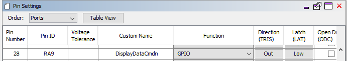
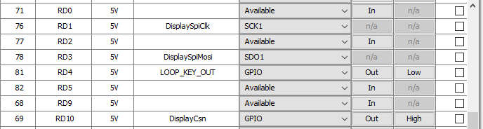
Here's a brief explanation of the latest hardware drawings.
- Display - The display is driven in 8 bit SPI mode using SPI hardware in the PIC32MZ. In 8 bit SPI mode,
the required interface includes MOSI, SpiClk, CSn, and DisplayDataCmdn. DisplayDataCmdn is held low during a command byte. A typical command sequence consists of the
following:
- Chip Select Low
- DisplayDataCmdn low
- 8 bit command over SPI
- DisplayDataCmdn high
- One or more 8 bit parameters over SPI
- Chip Select High
To avoid haing to wait around for SPI transmissions, a 16 bit wide FIFO is used. The 8 lsb carry SPI data while the high 8 bits carry the state of the chip select and command bit.
Data is put into the display FIFO without waiting for the SPI hardware. The main loop polls the SPI hardware and the display FIFO. When there is data in the FIFO and the SPI hardware
is ready, a 16 bit word is pulled from the FIFO and the appropriate information sent to the display.
- Loop Sense - An H11AA1 opto coupler detects loop current. The resistor across the LEDs diverts half the current so the LED current is 30 mA. The loop sense opto is in series
with the loop key SSR. The use of the opto and SSR allows the TU to be placed in the 60 mA current loop anywhere without regard to loop polarity. When there is loop current, LoopSense (RD14)
is pulled low. This is sensed by the code driving the AFSK generator and the code driving the software UART.
- Audio Bus Interface - My HF transceiver (SEA245) uses a "tristate" audio bus between the transceiver and the control head. This balanced audio
line is driven with receive audio during receive (PTT high) and with transmit audio during transmit (PTT low). Separate audio transformers are included in the TU to allow use with
transceivers that have separate receive audio output and transmit audio input. With the (SEA245), the left side of the two transformers are
connected in parallel. The top transformer in the drawing is not terminated, so it presents a high impedance to the audio line. The audio is biased up to Vcc/2, then presented to the AN4
analog to digital converter input on the PIC32MZ. There, the audio is sampled at 8 kHz, 12 bits per sample for demodulation. The bottom transformer drives the audio bus with transmit audio.
The AFSK Out comes from low pass filtered PWM (shown on the next drawing page). That audio is biased up to Vcc/2 (+1.65V). The other side of the transformer winding goes through a 1 uF DC
blocking capacitor to AfskOutEnn, RD15, on the PIC32MZ. That pin is programmed to be an open drain output. When programmed high, the pin floats, so there is no current through the transformer.
This disables transmit audio and unterminates the transformer so it does not load the bus. When AudioOutEnn is set low, current is allowed to pass through the transformer, so low impedance
AFSK audio is put on the audio bus. Use of the open drain output avoided the need for an analog switch or relay to switch the audio output between a high and low impedance state.
- AFSK Output - The PIC32MZ generates 80 kHz PWM on RE8. The duty cycle is changed at an 8 kHz rate to output audio. This is normally AFSK audio from the software
direct digital synthesis code, but can also output signals (AC or DC) from various parts of the code. The scope photos above are from this output. Originally, the PWM was changed to analog
with just a 4 kHz active filter. However, the op amp did not handle the high PWM frequency well, so an additional RC filter was put in front of it.
- Loop Keyer - RD4 of the PIC32MZ drives a solid state relay to key the 60 mA loop. As mentioned above, this is put in series with the loop sense H11AA1 to allow keying and sensing
of loop current.
- PIC32MZ EF Curiousity Board - This drawing shows the interface connections between the Curiosity evaluation board and the above hardware.
- Software Block Diagram - This drawing shows a block diagram of the receive portion of the TU. Under software control, the AGC can be replaced with a limiter. The software largely
duplicates a typical analog terminal unit.
Software
The latest software updates, as shown here, are:
- smp_type - Throughout the code, the type for audio sample was changed from double to smp_type. This allows a single line (in main.h) to be changed to change the audio sample
type between double and float. On the PIC32MZEF, the use of double results in a slight increase of CPU utilization (from about 11% to 12%). Note that there are several library functions
that take arguments as doubles and return doubles. To allow for different smp_types, inputs to these functions are type cast to double, and the output is type cast to smp_type. If
smp_type is already a double, this results in type casting a double to a double. I suspect the compiler ignores the unnecessary type cast under this circumstance.
- AfskGen.c - This code watches the loop sense input and drives sets the direct digital synthesis frequency as appropriate. The comments in initialization indicate that
a data low pass filter is initialized, but it currently is not. See the Baudot Uart section for more information on this.
- BaudotUart.c - This code receives data from the loop current sensor, runs it through a software uart, converts to ASCII to drive a hardware UART for debug, and counts
characters (valid start bits) and framing errors (invalid stop bits). The ratio of bad stop bits to valid start bits is a simple measure of receive performance. This code is
called 8,000 times per second, the same as the DSP sample rate. Note that the loop is sampled for 125us in the center of each bit. The short sample time can result in errors if
there is noise on the signal. Here, I got perfect copy when the loop was keyed by the model 15, but a fair number of errors when the loop was keyed by the model 14 TD. The model
15 printed the 14TD without error. The distributor in the 14TD was pretty dirty. Cleaning it removed the errors received in the BaudotUart. As mentioned in the AfskGen.c section,
above, i intend to add a low pass filter between the loop sense input and the AFSK generator. This will remove key clicks due to the fast frequency transition. The PPF will also
drive this UART, which should make it more tolerant of dirty distributors.
- dds.c - The value of pi was changed from 355/113 (from my HP35 manual) to acos(-1.0) for improved accuracy.
- main.c - Provision was made to change mark and space frequency based on shift frequency. Mark hold was added. It watches for DiscrimOut (MarkDemodOut-SpaceDemodOut) to be
above a specified threshold. Whenever DiscrimOut is above the threshold, the mark hold timer is loaded with a timeout value. If this timer times out, the loop keyer is held in mark.
Upcoming Work
PTTn has been added to drive the transceiver PTT line. It is driven with a 5V tolerant open drain output. This will be driven by a "Keyboard Operated Relay" in the code. The KOR
samples the loop current and if it finds the loop is in space and the loop is not being keyed by the TU, PTTn will be pulled low. A timer will hold PTTn low for several seconds after
the last space. In addition, PTTn will drive the AFSK output when low. Since PTTn is open drain, this can be driven by either KOR or an external switch to ground.
I intend to add a command interpreter to the Baudot Uart. With an escape sequence, the TU will change from normal transmit/receive operation to command entry. Various options
can be set, such as shift, KOR enable and time, mark hold threshold, etc.